描述
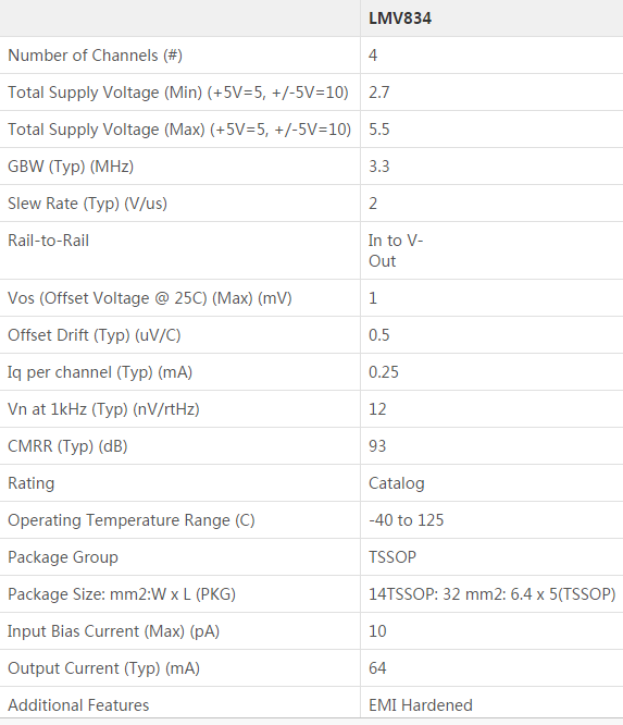
TI’s LMV83x devices are CMOS input, low-power operation amplifier ICs, providing a low input bias current, a wide temperature range of –40°C to 125°C, and exceptional performance, making them robust general-purpose parts. Additionally, the LMV83x are EMI-hardened to minimize any interference, making them ideal for EMI-sensitive applications.
The unity gain stable LMV83x feature 3.3-MHz of bandwidth while consuming only 0.24 mA of current per channel. These parts also maintain stability for capacitive loads as large as 200 pF. The LMV83x provide superior performance and economy in terms of power and space usage.
This family of parts has a maximum input offset voltage of 1 mV, a rail-to-rail output stage and an input common-mode voltage range that includes ground. Over an operating range from 2.7 V to 5.5 V, the LMV83x provide a PSRR of 93 dB, and a CMRR of 91 dB. The LMV831 is offered in the space-saving 5-pin SC70 package, the LMV832 in the 8-pin VSSOP and the LMV834 is offered in the 14--in TSSOP package.
特性
Unless Otherwise Noted, Typical Values at
TA= 25°C, V+ = 3.3 V
Supply Voltage 2.7 V to 5.5 V
Supply Current (per Channel) 240 µA
Input Offset Voltage 1-mV Maximum
Input Bias Current 0.1 pA
GBW 3.3 MHz
EMIRR at 1.8 GHz 120 dB
Input Noise Voltage at 1 kHz 12 nV/√Hz
Slew Rate 2 V/µs
Output Voltage Swing Rail-to-Rail
Output Current Drive 30 mA
Operating Ambient Temperature Range –40°C to
125°C
中广芯源专业电源方案系统服务商,小家电电源方案,工业辅助电源方案,智能LED调光电源驱动IC,功率:30W以内,有针对性的方案提供产品特色降低系统成本,提高设计灵活性。
1 220V降压12V/24V输出功率更大以适应更高功率的应用
2 非隔离电路无需变压器,外围电路更简单
3 节约外围元件成本
4 完全集成的缓启动电路降低了器件的应力及输出电压过冲
5 外部电路实现精确的限流编程
6 更宽的占空比实现更高的输出功率,同时可以使用更小尺寸的输入滤波电容
7 输入欠压(UV)检测可以防止关机时输出的不良波动
8 输入过压(OV)关断电路提高了对输入浪涌的耐受力
9 具有输出短路保护,开路保护功能
高精度带宽 4.5M 运算放大器 AD8551(单通道),AD8552(双通道),AD8554(四通道)
应用领域:
温度测量
压力传感器
精密电流传感
电子秤
应变计放大器
医疗仪器
热电偶放大器
手持式测试设备